- 您现在的位置:买卖IC网 > Sheet目录1994 > DS3106LN+ (Maxim Integrated Products)IC TIMING LINE CARD 64-LQFP
DS3106
13
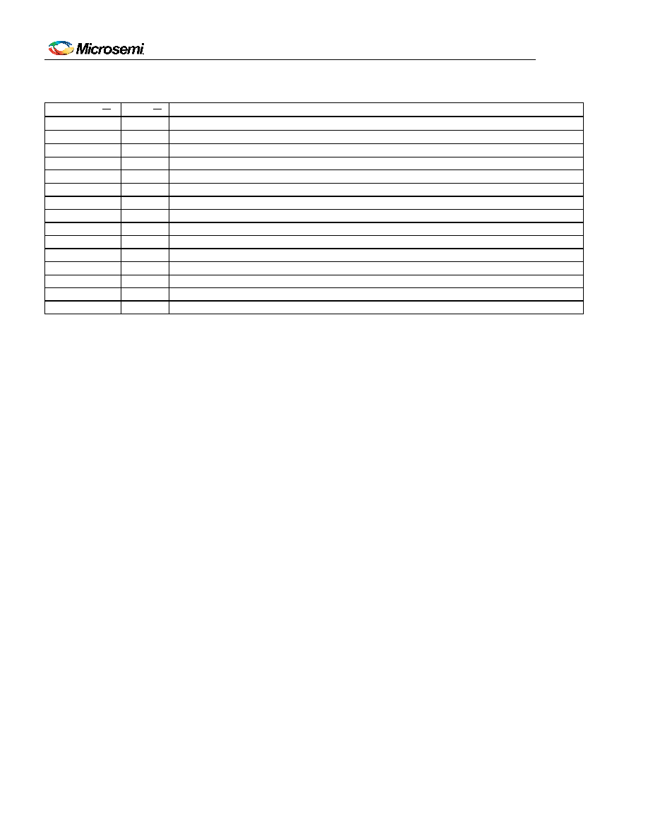
Table 6-6. Power-Supply Pin Descriptions
PIN NAME
TYPE
PIN DESCRIPTION
VDD
P
Core Power Supply. 1.8V
±10%.
VDDIO
P
I/O Power Supply. 3.3V
±5%.
VSS
P
Ground Reference
AVDD_DL
P
Power Supply for OC6 Digital Logic. 1.8V
±10%.
AVSS_DL
P
Return for OC6 Digital Logic
VDD_OC6
P
Power Supply for Differential Output OC6POS/NEG. 1.8V
±10%.
VSS_OC6
P
Return for LVDS Differential Output OC6POS/NEG
AVDD_PLL1
P
Power Supply for Master Clock Generator APLL. 1.8V
±10%.
AVSS_PLL1
P
Return for Master Clock Generator APLL
AVDD_PLL2
P
Power Supply for T0 APLL. 1.8V
±10%.
AVSS_PLL2
P
Return for T0 APLL
AVDD_PLL3
P
Power Supply for T4 APLL. 1.8V
±10%.
AVSS_PLL3
P
Return for T4 APLL
AVDD_PLL4
P
Power Supply for T0 APLL2. 1.8V
±10%.
AVSS_PLL4
P
Return for T0 APLL2
Note 1: All pin names with an overbar (e.g.,
RST) are active low.
Note 2: All pins, except power and analog pins, are CMOS/TTL, unless otherwise specified in the pin description.
PIN TYPES
I = input pin
IDIFF = input pin that is LVDS/LVPECL differential signal compatible
IPD = input pin with internal 50k pulldown
IPU = input pin with internal 50k pullup
I/O = input/output pin
IOPD = input/output pin with internal 50k pulldown
IOPU = input/output pin with internal 50k pullup
O = output pin
O3 = output pin that can be placed in a high-impedance state
ODIFF = output pin that is LVDS/LVPECL differential signal compatible
P = power-supply pin
Note 3: All digital pins, except OCn, are I/O pins in JTAG mode. OCn pins do not have JTAG functionality.
发布紧急采购,3分钟左右您将得到回复。
相关PDF资料
DS3231MZ+
IC RTC I2C 8SOIC
DS3231SN#T&R
IC RTC W/TCXO 16-SOIC
DS3232MZ+
IC RTC W/SRAM I2C 8SOIC
DS3232SN#T&R
IC RTC W/TCXO 20-SOIC
DS3234S#
IC RTC W/TCXO 20-SOIC
DS32C35-33#T&R
IC RTC ACCURATE I2C 3.3V 20-SOIC
DS3911T+
IC DAC 10BIT I2C QUAD 14TDFN
DS4000KI/WBGA
IC OSC TCXO 19.44MHZ 24-BGA
相关代理商/技术参数
DS3107FP000
制造商:Thomas & Betts 功能描述:30A,CON,2P3W,MG,107,125V
DS3107FRAB0
制造商:Thomas & Betts 功能描述:30A,REC,2P3W,MG,107,AB0,125,SC
DS3107MP000
制造商:Thomas & Betts 功能描述:30A,PLG,2P3W,MG,107,125V
DS3107MP00K
制造商:Thomas & Betts 功能描述:30A,PLG,2P3W,MG,107,125V,CC
DS3107MR000
制造商:Thomas & Betts 功能描述:30A,NLT,2P3W,MG,107,125V
DS3107MRAB0
制造商:Thomas & Betts 功能描述:30A,NLT,2P3W,MG,107,AB0,125V
DS3108A14S5S621
制造商:Amphenol Corporation 功能描述:
DS3108A14S6S
制造商:Amphenol Corporation 功能描述: